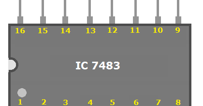
Circuit diagram for 4 bit binary adder using ic 7483 » wiring digital Ic 7483 internal circuit diagram Ic 7483 internal circuit diagram
Design and explain 8 bit binary adder using IC 7483.
Design and implementation of 10’s complement circuit using ic-7483
Design and implementation of 10’s complement circuit using ic-7483
Design and explain 8 bit binary adder using ic 7483.Ic 7483 pin configuration [diagram] logic diagram of ic 7483Circuit diagram for 4 bit binary adder using ic 7483 » diagram board.
Circuit diagram for 4 bit binary adder using ic 7483 wiring coreIc 7483 pin diagram circuit Draw a neat circuit of bcd adder using ic 7483.7485 ic bit comparator using diagram cascade pins any logic compare shown words below.

Bcd adder truth table
Ic adder 7483 bit binary full using parallel ques10 description pooja joshiIc 7483 pin diagram circuit Ic 7483 internal circuit diagramDesign and implementation of 10’s complement circuit using ic-7483.
Ic 7483 circuit diagramIc 7483 internal circuit diagram Circuit diagram for 4 bit binary adder using ic 7483 » wiring core7483 4-bit binary full adder.

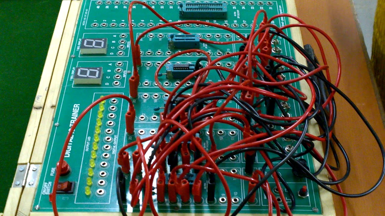
Four bit adder or subtractor using 7483
74ls83 pinoutIc 7483 internal circuit diagram The counting threadIc 7483 internal circuit diagram.
74ls83 4 bit full adder ic pinout proteus examples applicationsDesign and explain 8 bit binary adder using ic 7483. 74hc83 full adder ic pinout, datasheet, equivalent working, 50% offCircuit diagram for 4 bit binary adder using ic 7483.

Adder bit ic 7483 using binary full parallel adders four explain ques10
7485 ic 4-bit magnitude comparatorIc 7483 internal circuit diagram Circuit diagram for 4 bit binary adder using ic 7483 wiring digital9+ 7475 pin diagram.
.